

Getting Technical and testing.
This month we will give some more details on the first system that is being built, a progress reports and some teaser details about our operating system that is being developed alongside the hardware.
In our last post we discussed the features, constraints and some decisions we had made toward designing the EDDIE system. Recalling that EDDIE is a system - made from numerous compatible and interchangeable components, we’ll present our starting system in some more detail this month.
We have three boards under test in this prototype system shown on the bench in the picture :
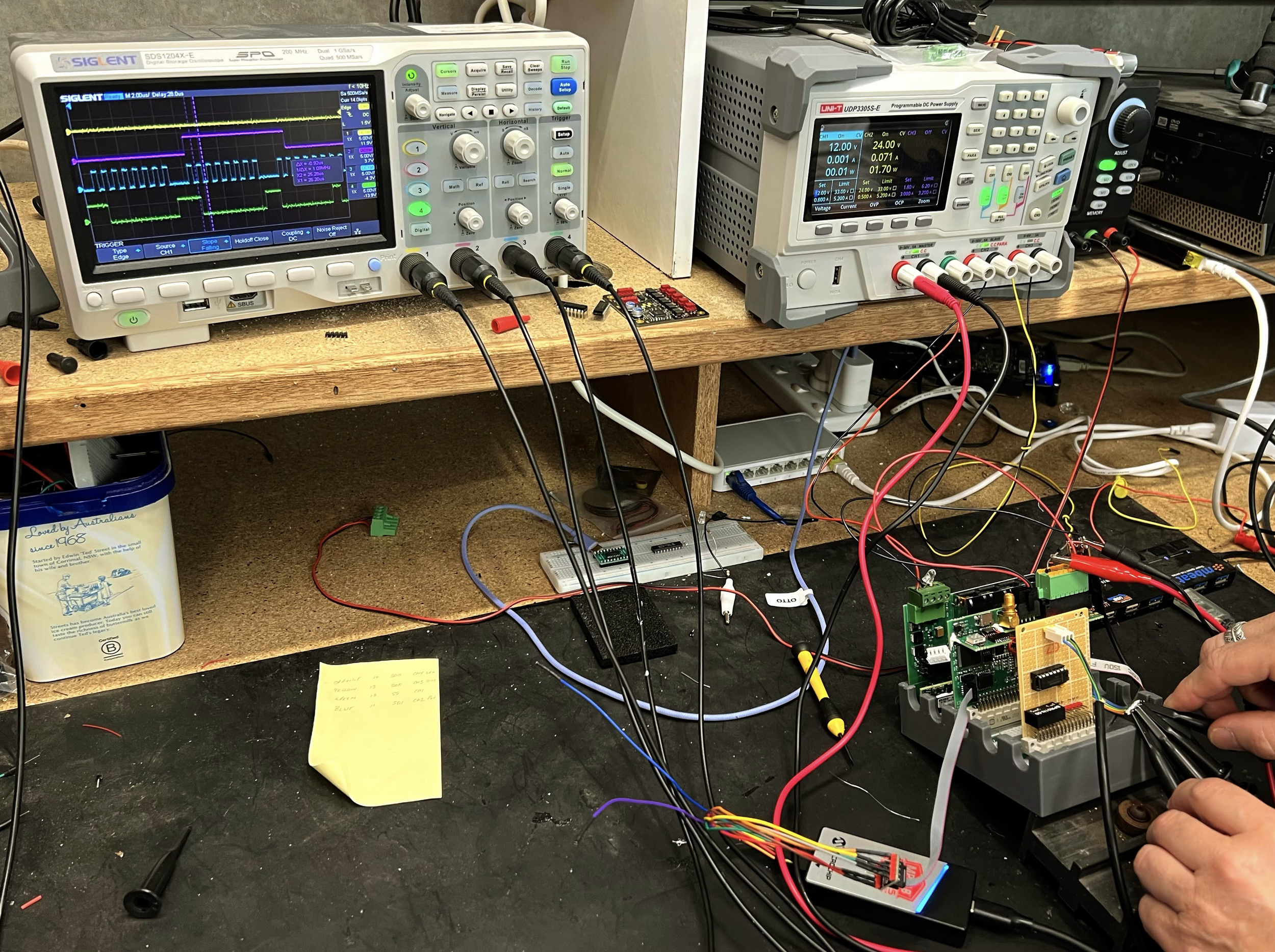
➡The backplane card
➡The Power/Ethernet support card
➡The CPU51 Card
(looking closely you will also see a small proto board at the front of the card rack. This is a simple 3.3V serial to RS-232 converter card. It helps us communicated from the host computer to the CPU when running our K4 environment)
To expand on the features and functions that are being tested have a look at the system block diagram. This is the system under test:
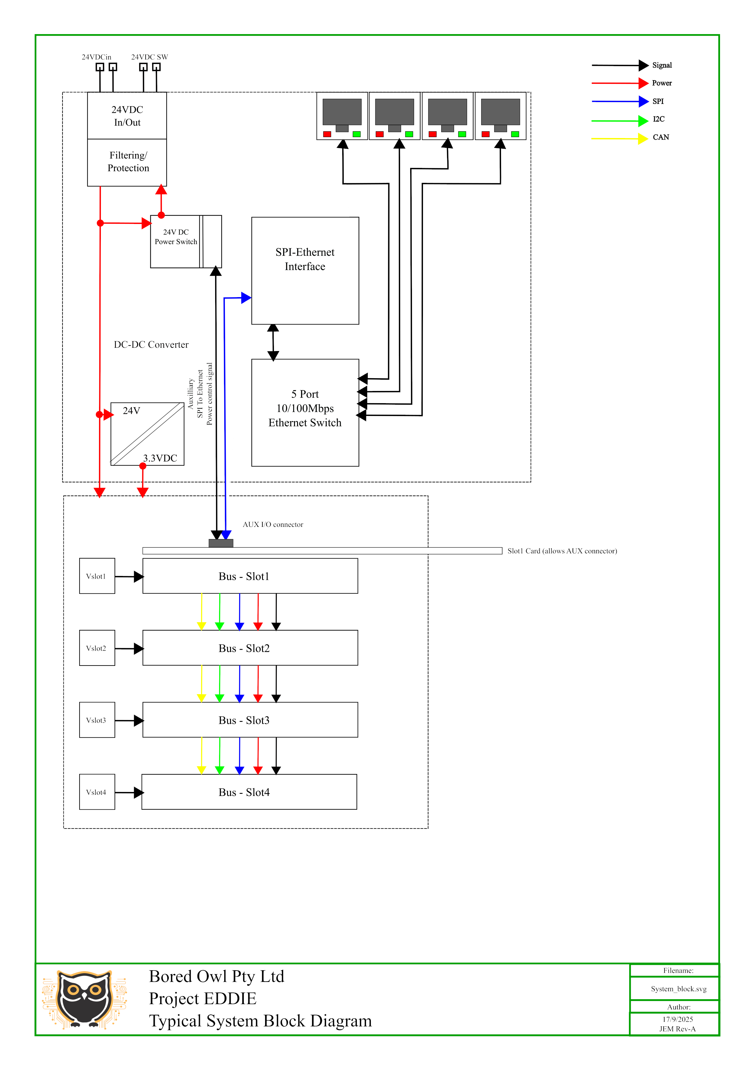
EDDIE System: System level block diagram
The incoming 24VDC power is filtered and protected. Protection is against reverse polarity connection and external over-voltage (>33VDC). Any excess current draw on the internal side - either through the 24VDC going out or due to an internal fault is fused by a poly-switch re-settable fuse.
This incoming power is then converted to 3.3VDC for logic circuitry. This 3.3VDC is galvanically isolated from the 24VDC coming in - meaning that neither the positive nor negative side of this supply is connected to the incoming power supply. This ensures that there can be no (or extremely minimal) current paths for surges and transients from the outside world into the logic. We have to be careful in the design of all the plug-in cards that this constraint is not violated.
The 3.3V power is provided to the SPI-Ethernet converter logic and to the ethernet switch that is on the interface board. It is also connected across to the backplane as power for the plug-in cards.
One learning from our testing has been that over-voltage disturbances on this power can cause significant damage across this entire system. Such over voltages are not likely in final manufactured systems - but still possible. The immediate problem is that simple inadvertent short circuits have had major impacts. To overcome this (and not shown in the diagrams), we have retrofitted a “crowbar” circuit to the supply. Such a circuit acts to short the supply when it exceeds 3.6VDC. This circuit can handle >2A and resets when the fault goes away.
The backplane card is mostly only interconnection. Initially in our design, each slot had a small serial EEPROM device connected to provide identification to the specific slot. It has turned out to be simpler to use a resistor divider network unique to each slot providing a slot voltage “Vslot” that the card can use when reporting its type and location. This is part of the software system used for configuration and will be discussed later.
Using the test bus, we are plugging the first CPU card in and testing it. This card is built around an ATSAMD51P20A CPU chip. This device offers enough serial ports (SPI, I2C and UART) as well as interfaces for CAN, QSPI flash memory and general purpose I/O.
The next block diagram illustrates the complete system built onto the revision A CPU card.
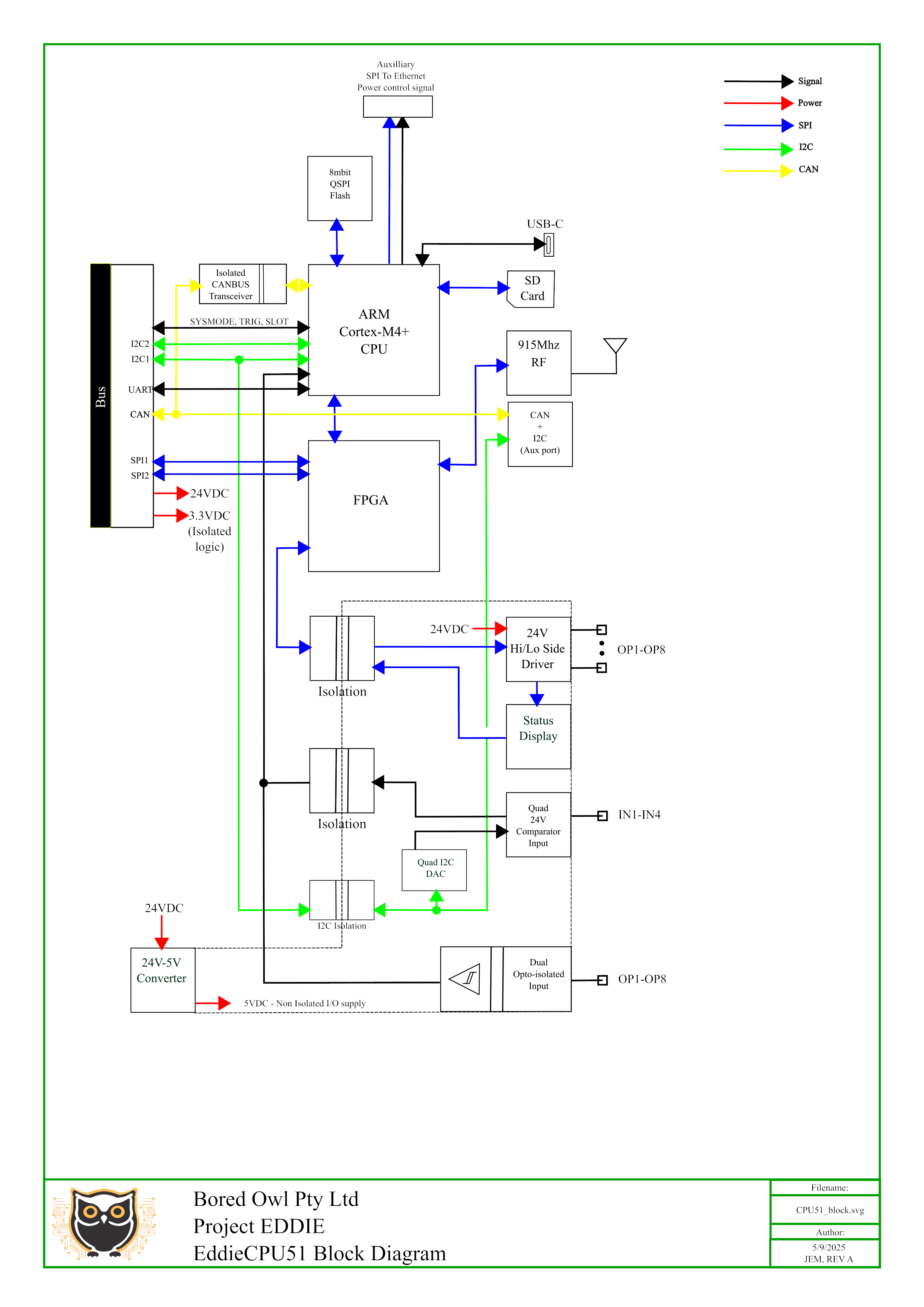
EDDIE System: CPU51 Block diagram
What this really means is that power has been applied, and work is underway to test the functionality of the first CPU51 card in a real rack. This has established that the system illustrated in these two block diagrams has been giving satisfactory results while undergoing testing:
The power/Ethernet card is providing 3.3V and the 24V power switch functions as required. The SPI Ethernet interface is yet to be tested.
The backplane is connected and the CPU card is plugged in. A small test card was bread-boarded (image at right). This card connects the CPU UART signal on the bus to an RS-232 serial port in our development computer.
The CPU card has been loaded with our “K4” language system. This is discussed below. It allows us to run tests by writing short programs that test sections of the CPU system.
The I/O on the CPU card is fully verified:
The comparator and monitor inputs are proven
The I2C comparator DAC is functional
The eight 24V output switches function,
The status display is working
The FPGA is switching SPI and UART signals to the bus
There is still the SPI-Ethernet, SD Card, QSPI Flash, USB, CAN, RF and actual operation with another bus card that must be verified.
There are however now a significant number of modifications on the card, mechanical issues and new ideas. (see the mess in the picture) We have decided to rework the card and the card will be rebuilt to a revision-B standard in the coming month. The fragility of the modifications may no be evident in these small pictures, but we have had to replace two CPU chips and three FPGA’s to get to this point. Building another revision A card was deemed to be less progress than the small cost of a PCB revision which will have no modifications.
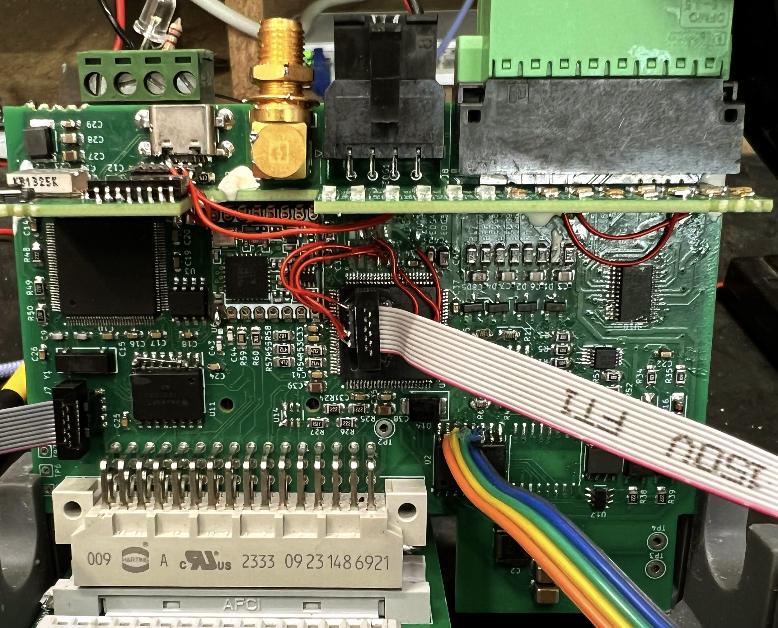
You don’t get everything right on the first go! EDDIE Rev A CPU51
The PCB revision will have more facilities for testing, mechanical improvements and a couple of new features. While this board is being manufactured, the SD card and QSPI software/hardware is expected to be developed and verified.
In our coming post, we will complete the content sent out in the third EDDIE newsletter and talk a bit about how we are using our K4 language on the CPU51 board, how it is being used in testing and its future in our EDDIE system.
Features and functions described in our blog posts are not final specifications. Products when made for sale will be published with official documentation and specifiactions that may differ from our aspirations during this development process.