

Probing questions
Our EDDIE-Probe Concept
In this post, we introduce EDDIE Probes. The concept of probes came about for a number of reasons:
We have a need for analog I/O quickly for an immediate application for EDDIE
Designing full analog cards is a relatively slower and more complex process than the simpler probe design we discuss here.
Bringing large quantities of wiring (especially arrays of sensors) into a centralised card box is cumbersome. Distributing the I/O at the point where it is required reduces the cabling.
Putting probes off of the backplane system un-burdens the backplane and makes slots available for higher power functionality.
Probes can and will be very diverse. We intend to have many variants and functions often mirroring higher density or higher performance full EDDIE cards. The probes we discuss here are to match our application. Even as this post gets published, there are plans for at least two more types.
The current work underway to build three external modules or “Probes”, will extend the I/O in an EDDIE system quickly for a specific application. The probes are designed to be general purpose (widely applicable) even though they are being used in this specific case.
The notion of the probes has developed in response to one of our first applications for the EDDIE system: Bored Owl is engaged in the design and manufacture of power LED drivers. This requires the characterisation of buck-boost power systems and PWM dimmers. EDDIE will be used to measure the voltage and current outputs of these power supplies while changing input voltage, load and operating parameters.
In essence, probes manage an I2C interface and sometimes a CAN interface with a local processor element. Power is conditioned locally and the analog front end is designed to suit a specific probe type:
At present we have three probe modules under development. Some of the designs are built up and pictured at the right.
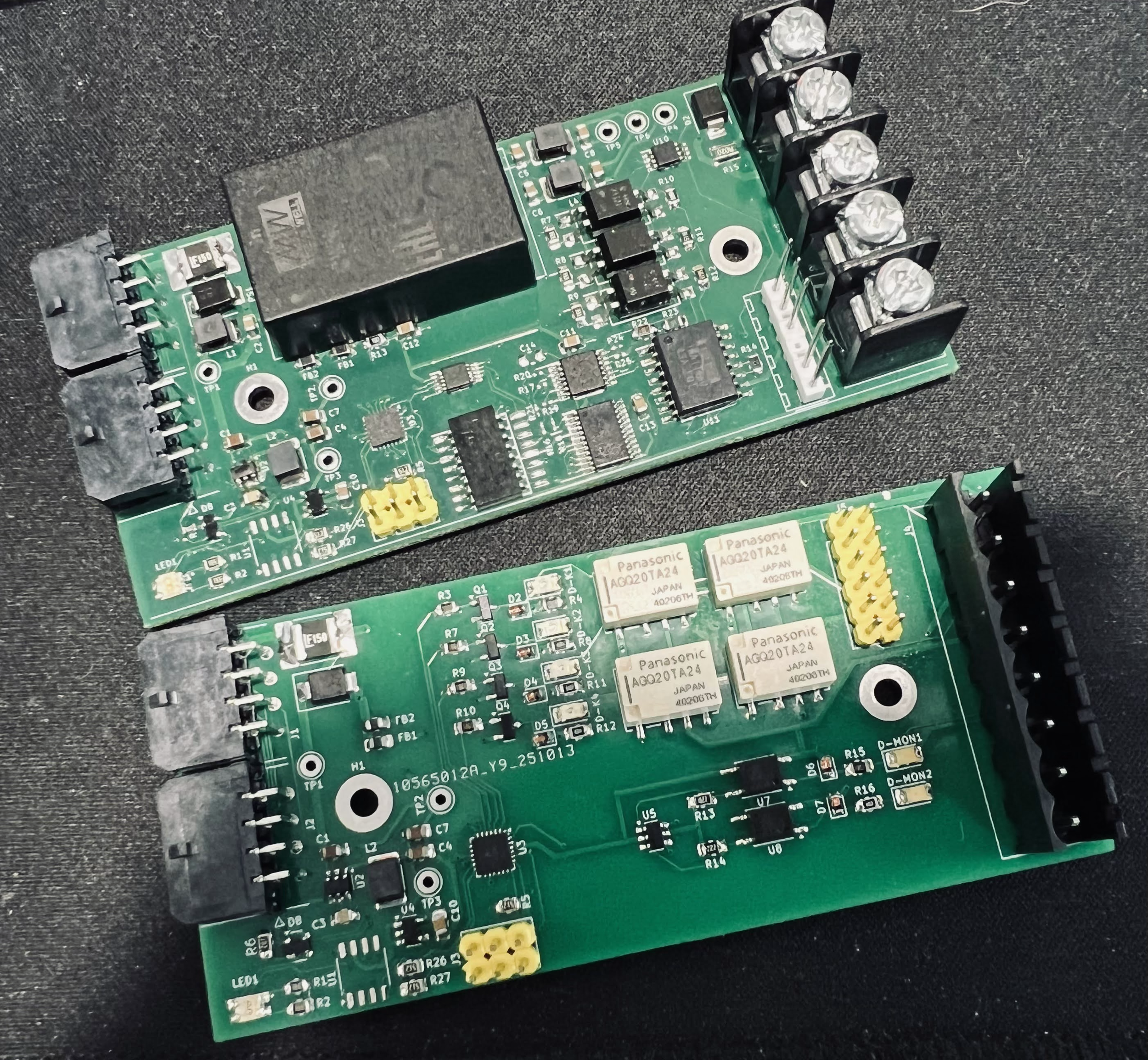
Two of our new probes as hand built prototypes
An analog I/O probe. This probe is intended to make high range and high resolution analog measurements. It has a 24bit ∑∆ ADC preceded by a programmable gain block with gains of 1/8, 1/4, 1/2, 1, 1.375, 2, 4, 8, 16, 32, 64 and 128. Coupled with a current sense amplifier and an instrumentation amplifier, this probe is designed to:
Measure a current of up to 2.5A (floating on up to +80VDC rails). Programmable gain enables minimum full scale current to be as low as 50uA at full resolution.
Measure the voltage across the current measurement input.
Measure a second differential voltage as high as +/-40VDC.
Measure temperature using a silicon sensor flying probe.
Measure an additional 0 .. +10V single ended voltage.
A programmable load. This probe can set a load (current sink to 0V) of 0 .. 2.5A with 12 bits of resolution. The load is on a separate heat sink assembly that can be liquid cooled and is temperature monitored. The probe can disconnect the load under remote control or overload/over-temperature conditions. An additional open-collector 24VDC output is also provided.
A relay output unit. This unit provides relay contact outputs (2A/24VDC). There are four relays, with normally open and normally closed contacts available. Additionally two terminal sets can be configured to monitor 24VDC switch signals as inputs.
Probes are based on a simple architecture suggested in the block diagram below:

Typical "EDDIE” probe block diagram
The block diagram is filled in according to the functions required. We are using ATSAMD11 and ATSAMD21 processors as the local processor (the bigger SAMD21 is used where CAN bus is supported). The I2C and optional CAN transceiver circuits are standard to all probes. Power conversion depends somewhat on the analog front-end requirements, conversion always supplies digital power to the local processor. Sometimes +ve/-ve and isolated supplies are needed by the analog circuits.
Within the EDDIE software environment, K4 will offer standard words (functions) and objects for communicating with probes. Probes will be discovered and enumerated automatically. This should allow a user to focus on the function of the I/O and not its interconnection.
Probes are intended to be easy to develop and deploy. They are also intended to offer a user of the EDDIE system and easy way to get the right I/O close to where they need it.
With probes added to the EDDIE system, what does a system start to look like now:
When we put all the new components together, we might make a system as depicted in the diagram:
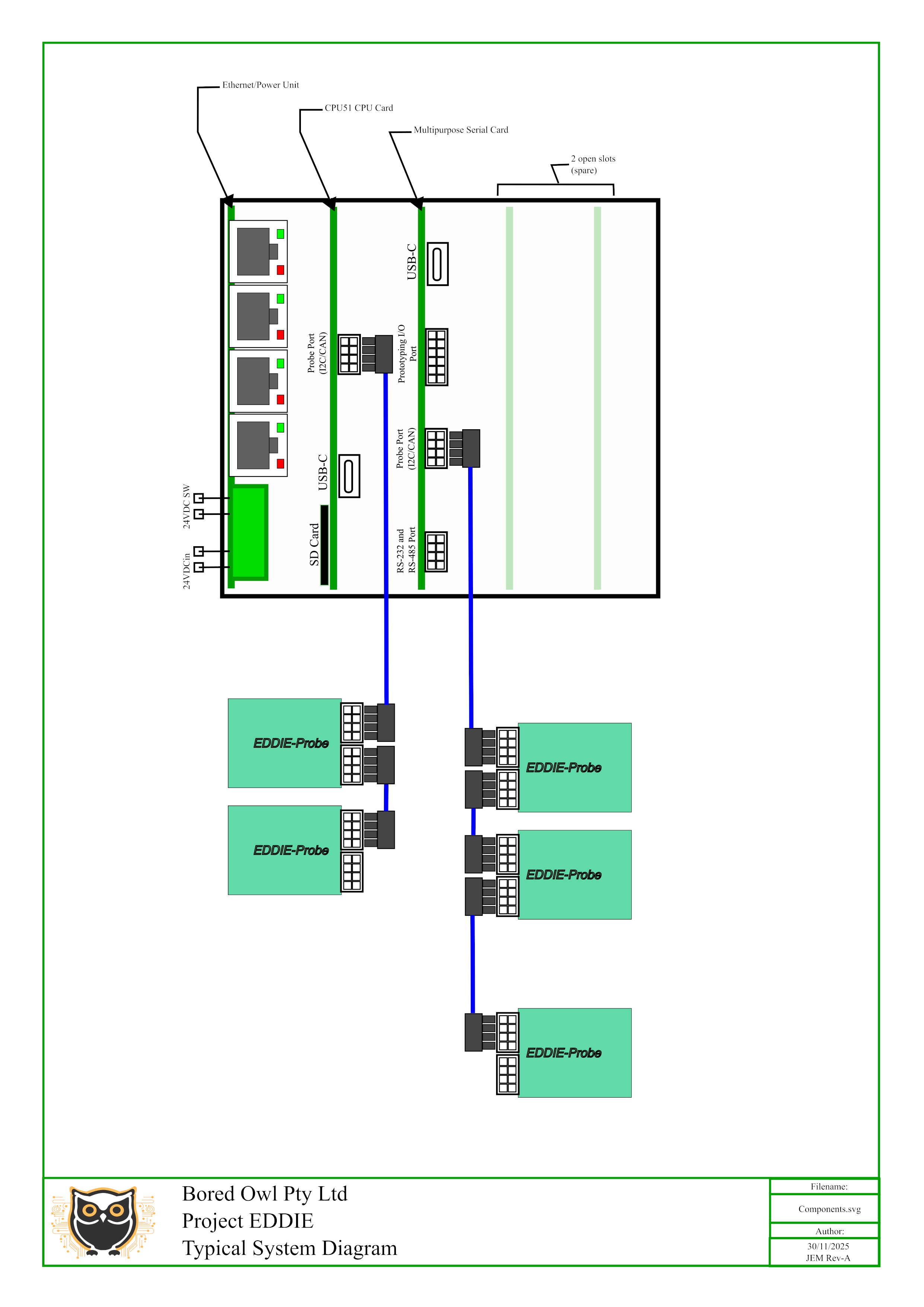
A typical EDDIE system using probes
This diagram shows the CPU card paired with the new serial card in the four-slot backplane. Onto this system we connect the probes.
Although there isn’t a hard specification yet, you can expect to add sixteen probe modules to each probe port. Using I2C probes, the modules may be up to 1.8m from the card cage. Using CAN bus, the distance (to the furthest node) could be 40-500 meters! depending on the transmission rates configured.
The diagram shows a typical configuration with five probes connected in two branches - one off the CPU card, and the other off a serial card:
Probes provide considerable expansion of an EDDIE system, without larger card cages. They also bring I/O signals closer to the target hardware and simplify wiring.