

The initial development phase:
Where are we at with Project Eddie?
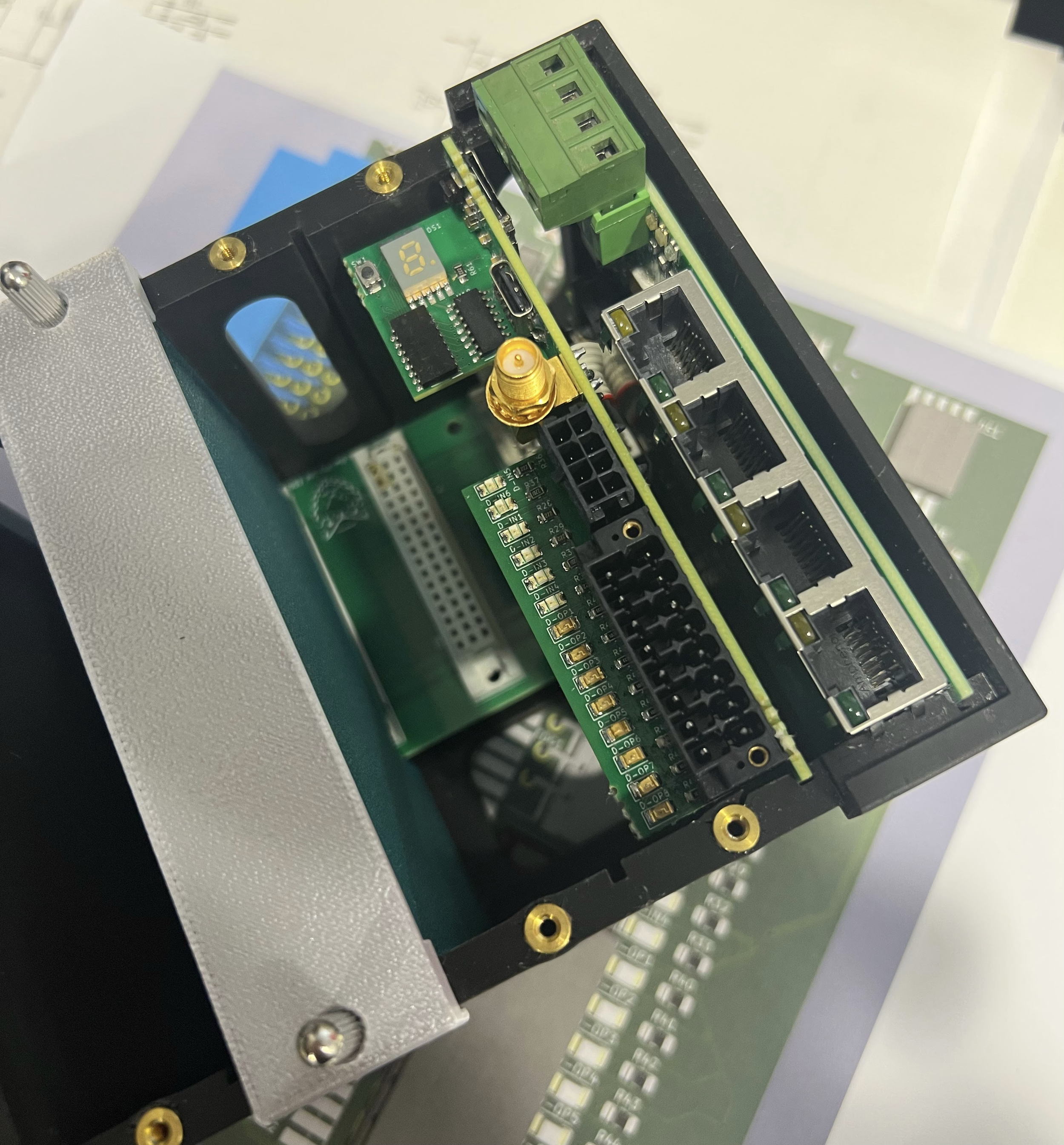
If you’ve been following our social media you’ll know we’ve received the bare CPU board and now its been loaded, so be sure to look through the photos later in the newsletter.
Initially, we have had to decide upon and design the physical outline for the product. This was done knowing that we needed space to accomodate power supplies and cards large enough to build the types of processors and I/O functions. There are trade-offs between the feature set of each board and the amount of PCB area needed to build those features. There is the enduring trade-off between the cost to build the card and the value it provides. There are also technical matters such as power consumption and dissipation and available connector configurations that have to be considered.
This stage (where we define the basic mechanical characteristics) of EDDIE is for us most desirably a single iteration stage. We need to get this right and not go back to scratch if having built the prototypes we find that it is difficult to make, awkward to use or unworkable in some other way.
A single, simple constraint became our main issue: Keeping our prototyping costs under control is high in our priorities. Prototyping actual circuit boards is a big impact on these costs. Typically from our experience three revisions of a circuit board might provide some semblance of series production. We are not designing most of these parts from circuits that have been prototyped in any way (breadboarded etc). That could be expected to add more revisions to the process. The simple constraint is that a 100x100mm two sided PCB can be prototyped for AU$5 in five off lots and takes only 3-4 days from design to physical item in our hands. We’ve decided to iterate the design in this format. (As the story will tell, we’ve had to contradict this in some places, but this is how we came to start designing our product envelope).
The product envelope.
Starting with the notion of a 100mm x 100mm envelope, what was the best card shape and size that we could come up with? One thing is always true to me when doing design like this: things are rarely completely new!
Firstly we knew the card must fit in a backplane, so we would have to design a backplane, then we can set our card in that backplane and build a card-frame around it.
This process has a precedent. The two images of some dusty boards I’ve kept from 10 years or more ago for a different product in a different lifetime. Things are rarely new: this design worked well and provides lots of useful clues for the EDDIE project.
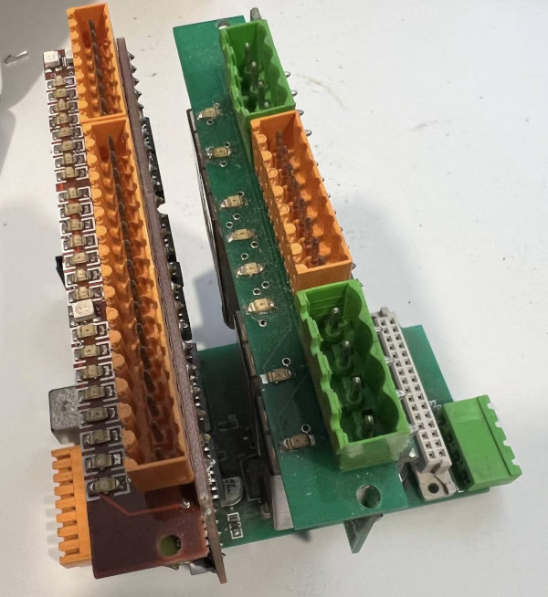
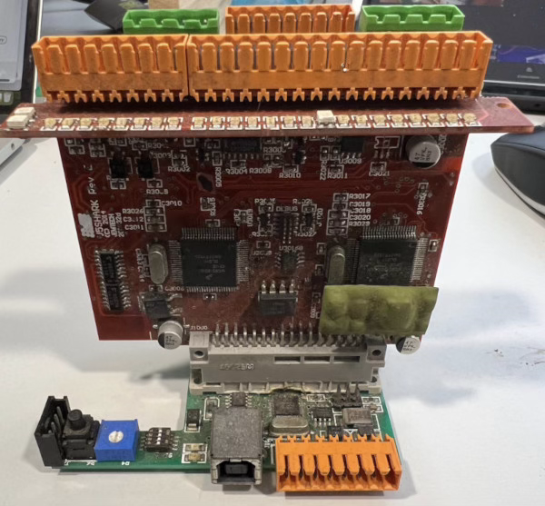
These are not EDDIE. These cards are 75mm high and 90mm wide - giving a good idea of what can be achieved in that area. (The green boards are two layer boards populated with micro-controllers and relays. The red board is a four layer design with two 112 pin TQFP microcontrollers with components on both sides)
The backplane in that case used half sized DIN41612 “Eurocard” connectors with 32 circuits available in each socket. Yes - Eurocard is a very old standard, but the parts are readily available, suit our manufacturing and are proven robust in the environments that we think the product will see.
Some early thinking about the nature of the bus that EDDIE would use had clearly shown that 32 circuits (from the previous desing) would probably be limiting (we’ll talk about the bus requirements in our next post). Using three row connectors 48 circuits are available and the connector size stays very similar.
Knowing the connector size and the board area allowed for a simple schematic for a backplane board to be drawn. A spacing between cards of 25mm was selected. The bus card could be fit onto a board of 100mm x 60mm. At this point I placed the components on the board artwork. (The PCB design is done using KiCAD 9 on an M1 MAC under OSX). Using KiCAD a 3D model of the board at this stage could be exported as an STL and then 3D printed:
Useful. The next step was to try various alternatives for the plug-in cards. Cards of 100x100, 100 high x 60 wide and 60 high by 100 wide. Some 3D models of those are illustrated below. Ultimately the 60mm x 100mm size was chosen with some extra area below the connector. This also leaves more board area in the 100mm x 100mm envelope if additional PCB parts were required in any design (eg vertical display boards).
Finally, a cage was built around the modelled cards using 3D CAD (OnShape) and several iterations yields the final result:


From this discussion and gallery, I hope you can see the beginnings of our product. In our up-coming blog entry I’ll start to talk more about the system architecture and how some of the first components are coming together.